
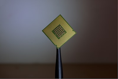
Intel's announcement that it has shipped the first logic chips made with High NA EUV extreme ultraviolet lithography marks a milestone in the semiconductor industry. This technology, developed in collaboration with ASML, allows transistors to be drastically reduced in size and integration density to be increased, resulting in more powerful and energy-efficient processors. To understand the magnitude of this advance, it is worth remembering that conventional EUV lithography, with a numerical aperture of 0.33, already represented a qualitative leap compared to previous techniques of immersion with deep ultraviolet light. Now, with High NA EUV (NA=0.55), unprecedented resolution is achieved, below 8 nanometers, paving the way for nodes of 2 nm and beyond. Intel has not only received the first machines, but has already manufactured functional wafers with this process, an achievement that demonstrates its ability to integrate and technological maturity.
This milestone is not just an incremental breakthrough: it represents a paradigm shift in chip manufacturing. The industry has been grappling with the physical limits of lithography for years, and High NA EUV is the answer to following Moore's Law. However, the road is not easy. High NA EUV machines are extremely complex and expensive – each unit is estimated to cost more than 300 million euros – and require adjustments to photoresist materials, masks and etching processes. Intel has invested billions in its factories in Oregon, Arizona and Ireland to stay ahead of the curve. The company has confirmed that these first logic chips are intended for qualification testing and that volume production will begin in the coming quarters, with the Intel 18A node as the main beneficiary.
From a technical perspective, the advantage of High NA EUV is that it allows patterns with a line width of 8 nanometers or even less, reducing the need for multiple exposures and simplifying the manufacturing flow. This not only improves the performance and energy efficiency of chips, but also reduces production costs in the long run. In addition, by being able to integrate more transistors in the same space, possibilities are opened for more complex architectures, such as 3D chips with vertical stacking. Companies such as Apple, AMD and Nvidia are attentive to this development, as their future designs depend on these technologies to maintain competitiveness.
In this context, semiconductor innovation drives the demand for advanced digital solutions. Companies that develop software for the simulation, design, and quality control of these chips need robust and scalable platforms. This is where Q2BSTUDIO, as a software and technology development company, offers differential value. Our team can create custom applications to manage lithography workflows, wafer data analysis, and process optimization, integrating AI tools to predict defects or improve performance. In addition, the custom software we design is tailored to the specific needs of each client, from semiconductor startups to large manufacturers.
The adoption of High NA EUV also has implications on IT infrastructure. The amount of data generated by lithography machines is colossal: each wafer produces terabytes of images and metrics. Processing and storing that information requires high-performance AWS and Azure cloud services , as well as cybersecurity solutions to protect intellectual property. At Q2BSTUDIO we help companies implement hybrid cloud environments that guarantee scalability and security, through business intelligence services that transform that data into actionable information. For example, power bi dashboards can visualize the efficiency of machines in real time, while AI agents automate anomaly detection.
On the other hand, artificial intelligence for businesses is revolutionizing the way manufacturing processes are optimized. Machine learning models can predict when an EUV machine needs maintenance, reducing downtime. At Q2BSTUDIO we develop AI agents that integrate with production line control systems, enabling autonomous decisions based on historical and real-time data. In addition, process automation becomes a key pillar to scale production without increasing human error. Our automation software can manage everything from wafer batch shipment to calibration of exposure parameters.
From a business perspective, Intel's leadership in High NA EUV is a sign that the semiconductor industry continues to invest in R+D despite bear cycles. For tech companies that rely on advanced chips, this advancement means they will be able to launch faster and more efficient products in the coming years. However, it also poses integration challenges: chip designers need EDA (Electronic Design Automation) tools that take advantage of the new lithography. Here, tailor-made software becomes indispensable. For example, a company developing quantum or AI chips may require a custom simulation system that calculates critical paths with nanometer accuracy.
Q2BSTUDIO also collaborates with firms in the sector to implement business intelligence services that help make strategic decisions. Let's imagine a manufacturer who wants to analyze the profitability of his different process nodes. With power bi and predictive models, it is possible to correlate the costs of High NA EUV machines with the performance of the chips, identifying bottlenecks. In addition, cybersecurity is critical when handling sensitive design data. We offer pentesting and security solutions to protect cloud and industrial environments, complying with regulations such as ISO 27001.
In conclusion, Intel's shipment of the first logic chips with High NA EUV is a milestone that will redefine processing power in the next decade. But beyond the technical achievement, this advancement requires an ecosystem of software and services to go along with it. At Q2BSTUDIO we are prepared to support companies in this transition, offering customized applications, cloud infrastructure, artificial intelligence and business intelligence solutions that maximize the return on this technological investment. The future of semiconductors is being written now, and the combination of cutting-edge hardware with intelligent software will make all the difference.